PCB Layout & Design Services In Gandhinagar, India
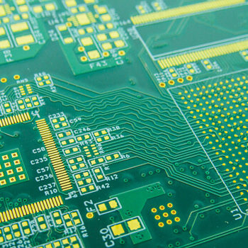
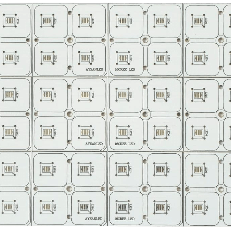
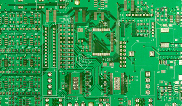
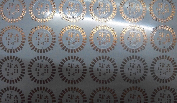
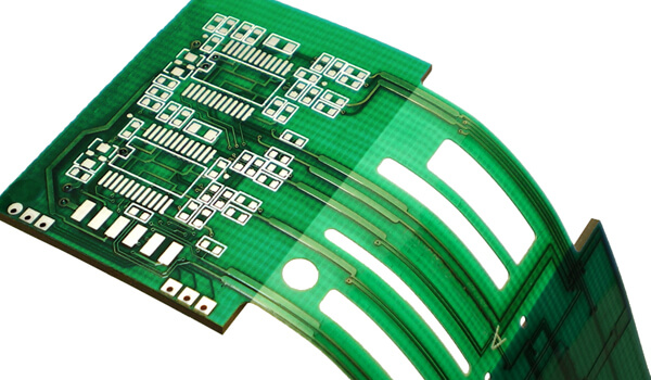
Introduction In the world of electronics, the layout and design of a PCB are critical factors that determine the performance, manufacturability, and cost-effectiveness of the final product. S B Electronics offers comprehensive PCB Layout & Design services that turn your conceptual electronic circuits into practical, optimized PCB designs ready for manufacturing.
Why Choose Our PCB Layout & Design Service
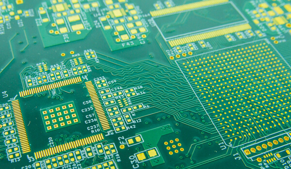
Our service stands out for its meticulous attention to detail, customization to client needs, and deep technical expertise. We work closely with our clients to ensure the PCB design meets their specifications, functionality requirements, and is optimized for manufacturing. Our team uses state-of-the-art design software and adheres to industry-leading practices to minimize issues and improve the overall quality of your project.
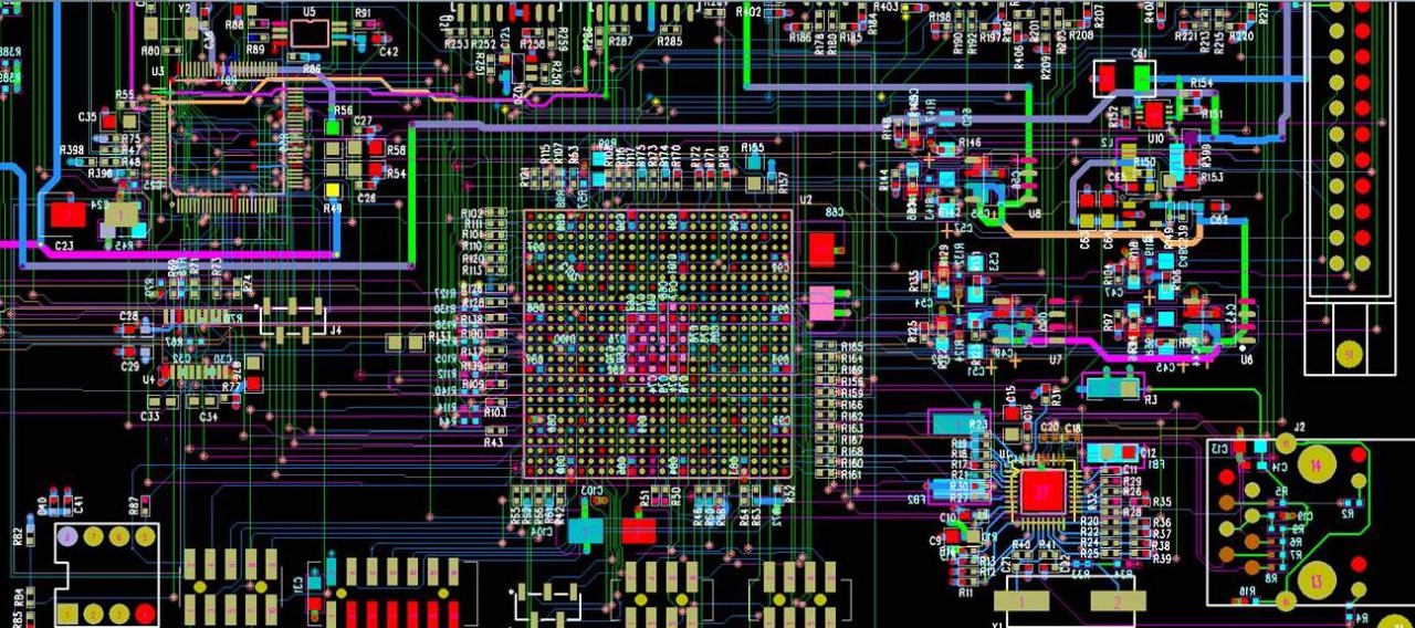
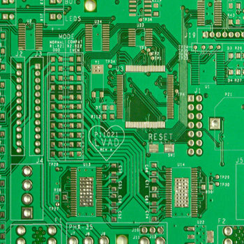
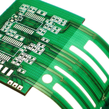
Capabilities and Features
Advanced Design Software
Design for Manufacturability (DFM) Checks
Thermal Management Solutions
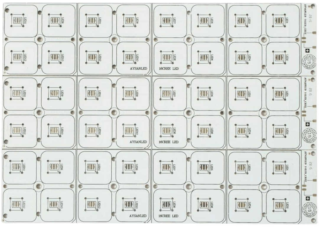
Expertise in Various Design Complexities
Signal Integrity Analysis
Conclusion S B Electronics PCB Layout & Design service is your gateway to transforming innovative ideas into functional, reliable, and manufacturable PCB designs. With our expertise, advanced tools, and commitment to quality, we ensure your projects are set up for success from the very start.