Capabilities · Datasheet
PCB manufacturing capabilities
- Layers
- 1–12
- Min. track / space
- 4 / 4 mil
- Min. drill
- 0.2 mm
- Express prototypes
- 24 h
On this page · 15 sections
Document
PCB manufacturing capabilities
Last updated
Scope
Rigid · multilayer · flex · assembly · stencils · sourcing
Quality
ISO 9001:2015 · IPC-A-600 · IPC-6012 · IPC-A-610 Class 2 & 3 · RoHS
Part A · Sheet 1 of 3Fabrication
§ 01–07 · Rigid · Multilayer · Flex · Finish · Drilling · Panels
01Fabrication
Rigid PCB fabrication
Our rigid line builds single-sided, double-sided PTH and NON-PTH, and multilayer boards, from one prototype to production volumes. The table is our published standard capability. Fine-line and on-request figures are not refused; they are built after an engineer has reviewed your data.
| Layer count | 1 to 12 layersSingle-sided, double-sided PTH / NON-PTH, multilayer |
|---|---|
| Base materials | FR-4 (Tg 150 °C / Tg 170 °C), FR-2, CEM-1, CEM-3, polyimide (flex) |
| Board thickness | 0.4 mm to 3.2 mm standard; 0.2 mm for thin rigid designs |
| Copper weight | 1 oz (35 µm) and 2 oz (70 µm) standard; 3 oz (105 µm) and heavier on request |
| Min. track / space | 6 mil / 6 mil standard; 4 mil / 4 mil fine-line |
| Min. drill diameter | 0.3 mm mechanical; 0.2 mm for fine-pitch designs |
| Surface finish | HASL (leaded), Lead-free HASL, ENIG, OSP |
| Solder mask | Green, Red, Blue, Black, White, Yellow — one or both sides |
| Silkscreen | White, Yellow, Black — top, bottom or both |
| Outline tolerance | ±0.15 mm as standard; ±0.1 mm on requestCNC routing |
| Impedance control | Controlled impedance, ±10% tolerance, with stack-up design support |
| Board size | Minimum 10 × 10 mm; maximum 500 × 600 mm (larger on request) |
| Panelisation | V-score, tab-routing (mouse bites) or a combination; rails, fiducials and tooling holes |
| Electrical test | 100% electrical test — flying probe or bed-of-nails fixture — plus AOI |
| Minimum order | No minimum order quantity — one prototype board upwards |
Which laminate should you specify?
FR-4 Tg 150 °C is the right default for most designs. Move to Tg 170 °C for lead-free assembly with several reflow passes, thick multilayer stacks or boards that run hot. FR-2, CEM-1 and CEM-3 keep cost down on single- and double-sided consumer boards, and polyimide is the base of every flex circuit.
Which copper weight?
1 oz suits most signal and logic boards. Choose 2 oz for power tracks and boards that shed heat through their copper; 3 oz and heavier are built on request. Heavier copper needs wider track and space, so set your design rules to match.
02Design check
Will my design fit?
Enter the figures from your fab drawing. Each is checked against the limits on this page: green is our standard process, amber is built on request after engineering review, and anything outside the published range goes to an engineer instead of being turned away.
Result
Fits our standard capability.
Single- and double-sided rigid boards like this can be priced online now, for dispatch in 3, 5, 7 or 10 working days.
- Layer count2 layers
StandardDouble-sided, PTH or NON-PTH.
Our published capability: 1 to 12 layers
- Board thickness1.6 mm
StandardInside our standard thickness range.
Our published capability: 0.4 mm to 3.2 mm standard; 0.2 mm for thin rigid designs
- Copper weight1 oz
StandardStandard copper weight.
Our published capability: 1 oz (35 µm) and 2 oz (70 µm) standard; 3 oz (105 µm) and heavier on request
- Min. track / space6 mil (0.152 mm)
StandardInside our standard process window.
Our published capability: 6 mil / 6 mil standard; 4 mil / 4 mil fine-line
- Min. drill0.3 mm
StandardInside our standard process window.
Our published capability: 0.3 mm mechanical; 0.2 mm for fine-pitch designs
- Board size100 × 80 mm
StandardInside our standard board size.
Our published capability: Minimum 10 × 10 mm; maximum 500 × 600 mm (larger on request)
- Surface finishLead-free HASL
StandardA standard finish on our line.
Our published capability: HASL (leaded), Lead-free HASL, ENIG, OSP
03Multilayer
Multilayer boards and controlled impedance
We laminate multilayer boards in 4, 6, 8, 10 and 12 layers on FR-4, with Tg 150 °C and Tg 170 °C laminates. Inner layers carry solid ground and power planes, which shorten return paths, cut EMI and leave the outer layers free for routing. Multilayer work is quoted per job after engineering review.
4 L
6 L
8 L
10 L
12 L
- 4 layers
- Typical layer roles: L1 SIG · L2 GND · L3 PWR · L4 SIG
- Signal, ground, power, signal: the usual step up from two layers. The planes cut EMI and free the outer layers for routing.
- 6 layers
- Typical layer roles: L1 SIG · L2 GND · L3 SIG · L4 SIG · L5 PWR · L6 SIG
- Two more routing layers for dense industrial controllers, DSP and communication modules.
- 8 layers
- Several planes and signal layers for mixed-signal designs, DDR memory and fast serial links.
- 10 layers
- Shielded signal pairs and isolated power domains for networking and telecom hardware.
- 12 layers
- Our highest standard count, for the densest routing and the most power domains.
Can you hold controlled impedance?
Yes — controlled impedance, ±10% tolerance, with stack-up design support. Put the target impedances, the controlled nets and their reference planes in the fab notes. We propose a stack-up — core and prepreg thicknesses, copper weights and trace widths — that meets them, and agree any change with you before production.
Keep the stack symmetrical about its centre and the copper balanced from layer to layer; it keeps the board flat through lamination and reflow. More on the multilayer PCB page.
04Flex
Flexible circuits
A flexible circuit is copper on polyimide film: it bends, folds and survives soldering temperatures where FR-4 would crack. We build single- and double-sided polyimide flex with polyimide coverlay on 12.5, 25 and 50 µm film, 0.1 mm to 0.3 mm finished. Every flex design is reviewed and quoted individually.
| Construction | Single- and double-sided polyimide flex with polyimide coverlay |
|---|---|
| Polyimide film | 12.5, 25 and 50 µm polyimide film |
| Finished thickness | 0.1 mm to 0.3 mm finished flex thickness |
| Min. track / space | 4 mil / 4 mil in the flex area |
| Min. drill | 0.2 mm laser; 0.3 mm mechanical |
| Outline tolerance | ±0.1 mm laser-cut; ±0.15 mm die-cut |
| Stiffeners | FR-4 and polyimide stiffeners; PSA backing on request |
| Surface finish | ENIG and lead-free finishes |
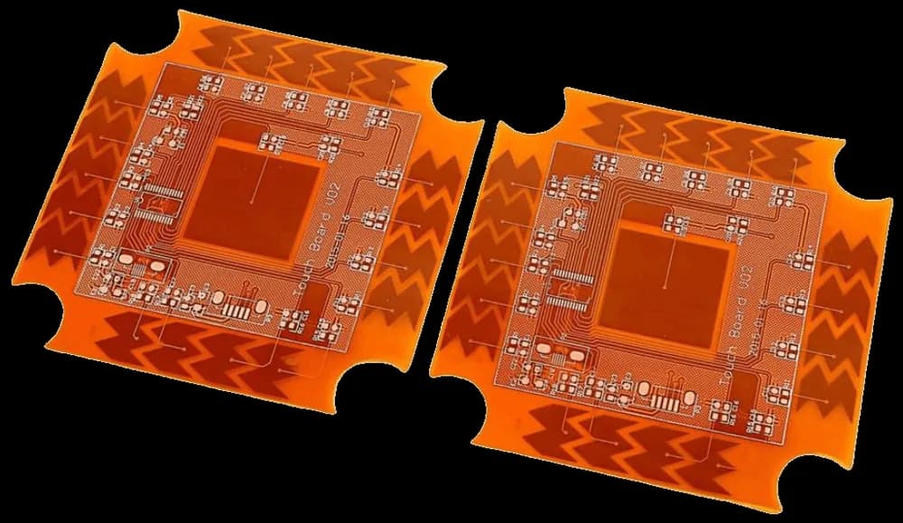
What to mark on a flex drawing
- Bend areas, and whether they flex once at installation or continuously in use
- Stiffener positions and material under connectors and components
- Coverlay openings and the finished thickness at the connector
- The bend radius you need, so we can check it against copper and layer count
05Finish & colour
Surface finishes and solder-mask colours
The surface finish protects exposed copper and decides how the pads solder; the mask colour is mostly cosmetic but changes how easily a board can be inspected. We offer HASL (leaded), lead-free HASL, ENIG or OSP, 6 mask colours and 3 legend colours. Try the combinations on our own demo board.
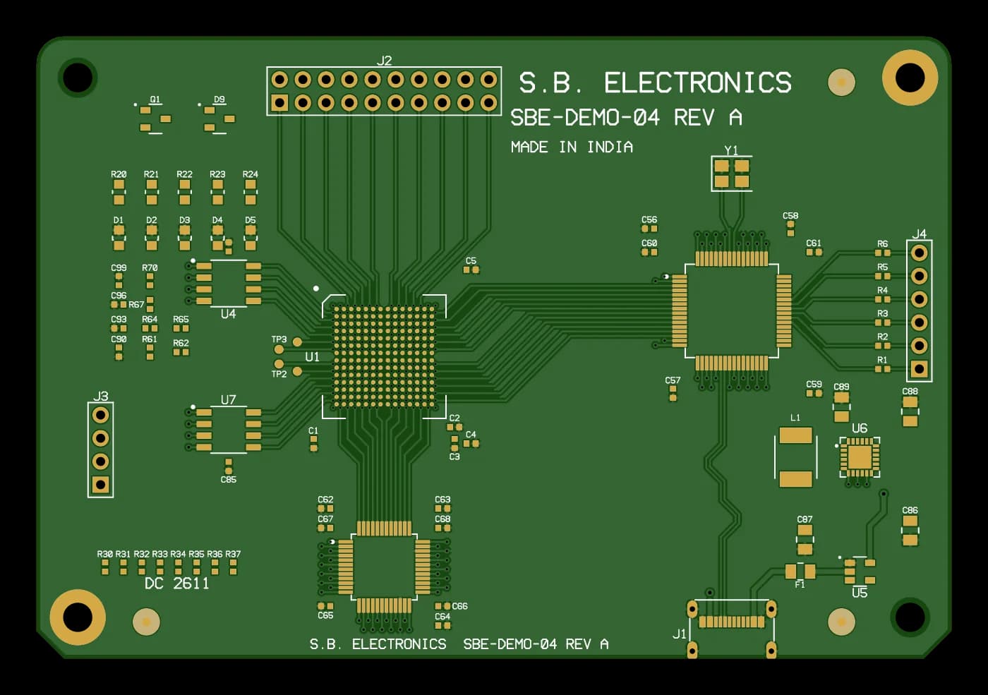
Mask goes on one or both sides; the legend prints on the top, the bottom or both. Mask colour does not change how the board performs electrically — only how it looks and how easily it can be inspected.
- Green mask
- The default. Highest contrast for optical inspection and the most forgiving process.
- ENIG
- Electroless nickel under a thin immersion gold. Dead-flat pads for fine-pitch QFP, QFN and BGA parts.
Which surface finish should you choose?
| Finish | Surface | Lead-free | Best for | Watch for |
|---|---|---|---|---|
| HASL (leaded) | Domed solder coat | No | Through-hole, hand soldering, general-purpose boards | Uneven on fine-pitch pads; not for RoHS products |
| Lead-free HASL | Domed solder coat | Yes | General SMT and through-hole; RoHS builds | Less flat than ENIG under fine-pitch QFP and BGA |
| ENIG | Flat nickel under gold | Yes | Fine-pitch QFP, QFN and BGA; flat contact pads | Costs more than HASL |
| OSP | Flat organic film on copper | Yes | SMT reflow on short production cycles | Limited reflow passes; assemble soon after delivery |
06Drilling & tolerance
Drilling, annular ring and tolerances
Mechanical drilling goes down to 0.3 mm as standard and 0.2 mm for fine-pitch designs. Leave at least 0.15 mm of annular ring around drilled holes so drill position tolerance never breaks out of the pad. Outlines are CNC-routed to ±0.15 mm, or ±0.1 mm on request.
| Limit | mm | mil |
|---|---|---|
| Track / spacestandard | 0.152 | 6 |
| Track / spacefine-line | 0.102 | 4 |
| Drillstandard | 0.3 | 11.8 |
| Drillfine-pitch | 0.2 | 7.9 |
| Annular ringminimum | 0.15 | 5.9 |
| Outlinestandard | ±0.15 | ±5.9 |
| Outlineon request | ±0.1 | ±3.9 |
1 mil = 0.001 in = 0.0254 mm
07Panels
Panelisation
Small boards are built and assembled in production panels, so they travel through every process as one piece. Boards are separated by V-score, tab-routing (mouse bites) or a combination, and every panel carries rails, fiducials and tooling holes. Send a single board and we design the panel, or send your own panel drawing.
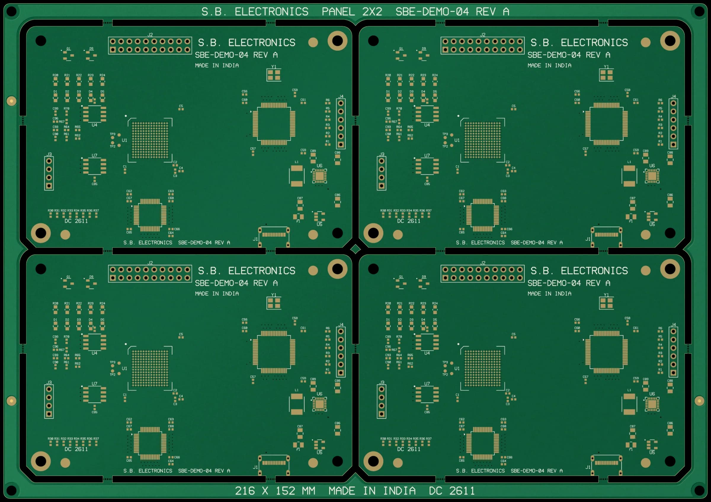
- 01Tooling hole on the rail. Locates the panel on drilling, test and assembly fixtures.
- 02Fiducial. A copper target the pick-and-place camera aligns to.
- 03Breakaway tab. Perforated (mouse-bite) tabs hold routed boards until depanelling.
- 04Routed slot. CNC-routed channel that frees the board outline, curves and all.
FIG. 07SBE-DEMO-04 in a 2 × 2 production panel, rendered from its panel Gerbers.
V-score
A V-groove cut from both faces leaves a thin web, and boards snap apart along straight lines. Fast and clean for rectangular outlines.
Tab-routing
Boards are routed to shape and held by perforated tabs. Use it for curved outlines and connectors that overhang the edge.
Combination
V-score where the edges are straight, tabs where they are not — common on mixed panels.
Part B · Sheet 2 of 3Test, assembly & services
§ 09–12 · Test · Assembly · Stencils · Sourcing
08Test & inspection
Electrical test and inspection
Every bare board is tested before it ships: 100% electrical test — flying probe or bed-of-nails fixture — plus AOI. AOI scans each etched layer against your data, the electrical test checks every net for opens and shorts, and final inspection signs boards off against IPC-A-600 before packing.
The 13 production stages · inspection gates in gold
- 01CAMCAM & DFM review
- 02CNCCNC drilling
- 03PTHHole metallisation
- 04DRYDry film & imaging
- 05PLTCopper plating
- 06ETCEtching
- 07AOIAutomated optical inspection
- 08LPISolder mask
- 09FINSurface finish
- 10LEGLegend printing
- 11RTGRouting & V-scoring
- 12E-TElectrical test
- 13FQCFinal inspection
- AOIAutomated optical inspection
- Every etched layer is scanned against the design data for opens, shorts and nicks.
- E-TElectrical test
- 100% flying-probe or bed-of-nails test verifies every net for opens and shorts.
- FQCFinal inspection
- Final QC against IPC-A-600 acceptance criteria, then protective packing and dispatch.
Flying probe or fixture?
A flying-probe tester moves its needles across the board under program control, so it needs no fixture: right for prototypes and short runs. A bed-of-nails fixture contacts every test point at once and suits volume orders once it is built. We choose by quantity; you only supply the design data, plus an IPC-D-356 netlist if your CAD tool exports one.
E-test · flying probe
Bottom side
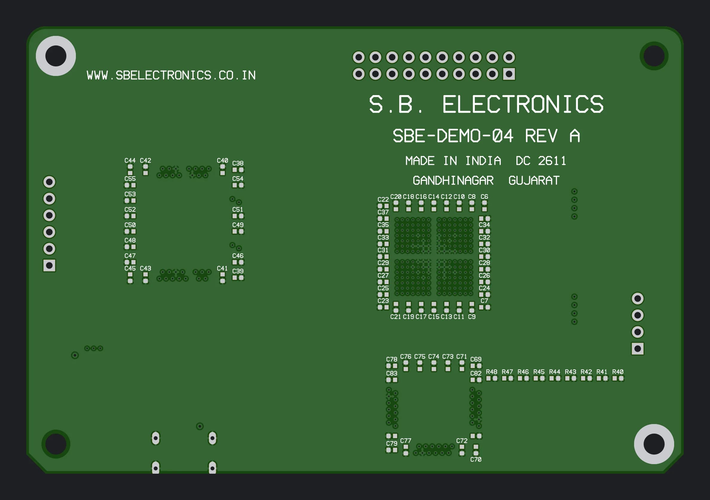
- Continuity
- Each net end to end · finds opens
- Isolation
- Net against its neighbours · finds shorts
09Assembly
PCB assembly
We assemble SMT, through-hole (THT) and mixed technology boards — full turnkey (we source the parts), partial turnkey or consigned (you supply them). Placement runs down to 0201 (imperial) passives and 0.4 mm minimum BGA ball pitch, with AOI at every stage and X-ray on BGA joints. Workmanship is to IPC-A-610 Class 2 standard, Class 3 on request.
| Technology | SMT, through-hole (THT) and mixed technology |
|---|---|
| Material model | Full turnkey (we source the parts), partial turnkey or consigned (you supply them) |
| Smallest component | 0201 (imperial) passives |
| Fine pitch | 0.4 mm minimum BGA ball pitch; QFN, QFP and fine-pitch ICs |
| Board size | 50 × 50 mm to 510 × 460 mm |
| Reflow | 8-zone lead-free reflow; leaded profiles on request |
| Soldering | Reflow, wave and selective / hand soldering |
| Inspection & test | AOI at every stage; X-ray for BGA; functional test on request |
| Workmanship | IPC-A-610 Class 2 standard; Class 3 on request |

Who supplies the parts?
Choose per order. The line and the inspection are the same in all three.
- Full turnkeyWe buy every part
- We review the BOM, buy every part and build the boards: one order, one delivery.
- Partial turnkeyShared
- You supply the parts you already hold — custom, costly or long-lead items — and we buy the rest.
- ConsignedYou supply every part
- Send the parts kitted against the BOM; we place, solder and inspect them on our line.
10Stencils
SMT stencils
Our stencils are laser-cut directly from your Gerber paste-layer data, in SUS304 stainless steel with electro-polished apertures for clean paste release. Foil thickness runs 0.08 mm to 0.2 mm, apertures go down to 0.08 mm at ±0.01 mm, and we supply them framed, frameless (foil), stepped and electroformed.
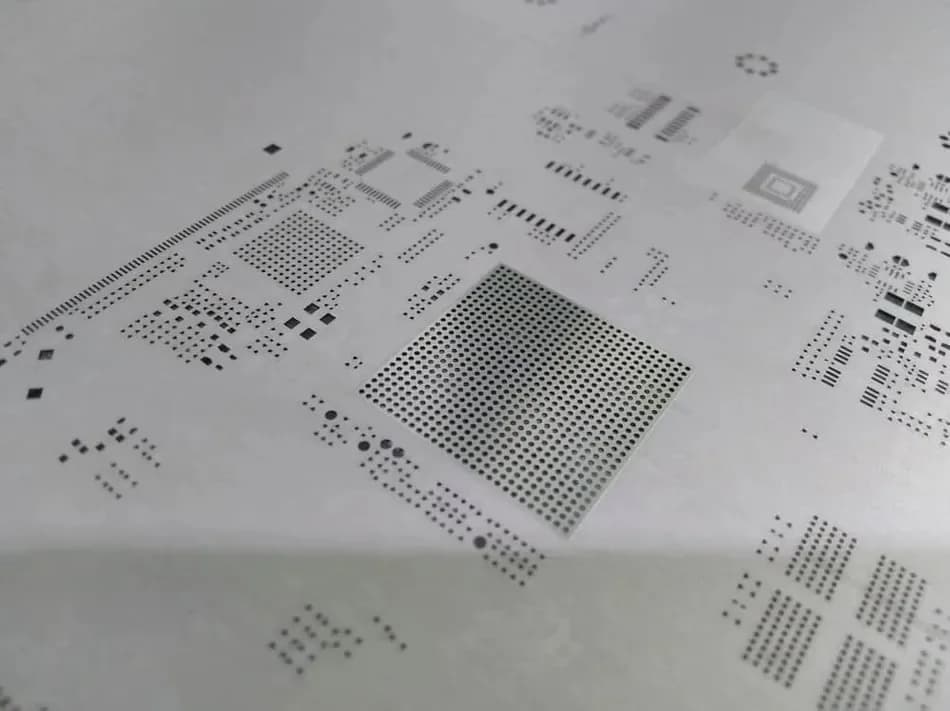
| Material | SUS304 stainless steel |
|---|---|
| Cutting | Laser-cut directly from your Gerber paste-layer data |
| Foil thickness | 0.08 mm to 0.2 mm foil |
| Min. aperture | 0.08 mm |
| Aperture tolerance | ±0.01 mm |
| Min. pitch | 0.5 mm QFP / fine-pitch |
| Formats | Framed, frameless (foil), stepped and electroformed |
| Aperture finish | Electro-polished apertures for clean paste release |
| Accepted data | Gerber (RS-274X), ODB++ and DXF |
Which foil thickness?
Match the foil to the finest pitch on the board. Thinner foils release paste cleanly from small apertures; thicker foils put down more paste for connectors and power pads. A stepped stencil does both on one foil.
PCB stencils in detail11Sourcing
Component sourcing
For turnkey assembly we buy from authorised distributors and manufacturers only — no grey-market or broker stock. Every part keeps its lot and date code, the BOM is reviewed before anything is ordered, and the parts arrive on our assembly line as a complete kit.
BOM review
BOM review for availability, lifecycle (EOL / NRND) and cost; drop-in cross-references proposed for approval.
Shortages and end-of-life parts surface on paper, before anything is bought.
Authorised buying
Authorised distributors and manufacturers only — no grey-market or broker stock.
Genuine parts, traceable back to their maker.
Traceability
Lot and date-code traceability on every part.
A suspect part can be traced back to its lot and date code.
Kitting
Kitted for assembly on our line.
The parts reach the line as one complete kit, checked against the BOM.
Part C · Sheet 3 of 3Ordering
§ 13–15 · Lead times · Files · DFM
12Lead times
How long does it take?
Simple, urgent prototypes can ship on a 24 h express turn. Single- and double-sided boards priced in the instant quote dispatch in 3, 5, 7 or 10 working days — choose the speed and the price follows. Multilayer, flex, assembly and stencil orders are quoted per job after engineering review.
Express
24-hour express for urgent simple prototypes.
Call or write before you order, so we can confirm the express turn for your design.
Ask for expressInstant quote
Dispatch in 3, 5, 7 or 10 working days, priced live in the instant quote.
Rigid single- and double-sided boards, 10 mm to 600 mm per side, 1 to 100,000 boards per line.
Open the instant quoteMultilayer & reviewed jobs
Quoted per job after engineering review.
We aim to answer requests for quote within 24 hours on working days, with the dispatch date.
Request a quoteWorking days run Monday to Saturday, and courier transit comes on top of the dispatch time. An order can be cancelled within 2 hours of ordering, before manufacturing starts.
13Design data
What files do we need?
For bare boards, send Gerber RS-274X (or X2) plus Excellon drill files; ODB++ accepted. For assembly, add a BOM (CSV / Excel, with manufacturer part numbers) and centroid / pick-and-place data. Zip everything into one archive and upload it with your quote, and put what the drawing does not show — material, thickness, finish, colours, impedance and IPC class — in a fab note.
- your-board.zip
- gerber/# Gerber RS-274X or X2, one file per layer
- copper_top.gbr
- copper_inner_1.gbr …# multilayer only
- copper_bottom.gbr
- mask_top.gbr · mask_bottom.gbr
- silk_top.gbr · silk_bottom.gbr
- paste_top.gbr# stencils and assembly
- outline.gbr# one closed board profile
- drill/# Excellon, plated and non-plated holes
- plated.drl
- non_plated.drl
- fab_notes.pdf# material, finish, colours, impedance
- bom.xlsx# assembly: with manufacturer part numbers
- centroid.csv# assembly: pick-and-place data
A fab note should state
- Base material and Tg
- Finished board thickness and copper weight
- Surface finish, mask and legend colours
- Impedance targets with their layers
- IPC class and any special tolerances
- Panel requirements, if you have them
14DFM
DFM design guidelines
Most production holds come from a handful of avoidable issues. Every order gets a CAM and DFM review before tooling is made; design to these rules and that review becomes a formality rather than a query.
- DFM-01
Annular ring
Keep at least 0.15 mm of copper around every drilled hole, so drill position tolerance never breaks out of the pad.
- DFM-02
Track and space
Route at 6 / 6 mil wherever the board allows; drop to 4 / 4 mil fine-line only where the routing needs it. Wider is cheaper and more robust.
- DFM-03
Copper to board edge
Pull copper back from the routed outline, and further still from V-score lines, so the cutter never exposes or burrs a plane.
- DFM-04
Solder-mask openings
Open the mask slightly larger than each pad, and do not leave slivers of mask between fine-pitch pads too narrow to stay bonded.
- DFM-05
Legend
Keep silkscreen text tall and bold enough to print legibly, and clear of pads, vias and mask openings.
- DFM-06
Drill data
Send the Excellon drill files with the Gerbers, with plated and non-plated holes in separate files and slots drawn as routed paths.
- DFM-07
Impedance
State impedance targets, the controlled nets and their reference planes in the fab notes, not only in the CAD rules.
- DFM-08
Panels
If you panelise yourself, put fiducials and tooling holes on the rails and keep parts clear of tab and V-score positions.
15Questions
Capability questions, answered.
Short answers to what engineers ask before sending data. Everything else: +91 96241 70703.
What is the minimum track width and spacing you can manufacture?
What is the smallest hole you can drill in a PCB?
What is the largest PCB size you can make?
How many layers can you build?
Do you manufacture controlled-impedance PCBs?
Which boards can I price in the instant online quote?
Is there a minimum order quantity for PCBs?
Which surface finishes and solder-mask colours do you offer?
Ready when your data is
Your design fits? Send the Gerbers.
Send the full data pack for multilayer, flex, assembly or stencils and an engineer replies with a reviewed quote. Single- and double-sided boards can be priced online in seconds.