G.I.D.C. Electronics Estate · Gandhinagar, Gujarat · Est. 2000
PCB manufacturer in India since 2000.
Single-sided to 12-layer, and flexible boards — fabricated, assembled and electrically tested in our own plant in Gandhinagar, Gujarat. One prototype or a production run, built to your data and dispatched across India.
Instant online price for rigid 1–2 layer boards. Multilayer, flex and assembly get a quote reviewed by an engineer — we aim to answer within 24 hours on working days.
- Layers
- 1–12
- Min. track / space
- 4 / 4 mil
- Surface finish
- HASL · LF-HASL · ENIG · OSP
- Electrical test
- 100%every board
- Express prototypes
- 24 h
Certification and standards
- CertifiedISO 9001:2015Quality management system for PCB design, manufacture and sales
- Bare boardIPC-A-600 · 6012Acceptance criteria and qualification for rigid printed boards
- AssemblyIPC-A-610Workmanship to Class 2 as standard, Class 3 on request
- Every board100% E-testFlying probe or bed-of-nails fixture, every net, before packing
- Lead-freeRoHSLead-free HASL, ENIG and OSP finishes for RoHS-compliant builds
- GandhinagarSince 2000One plant in the G.I.D.C. Electronics Estate, Sector-25
01In numbers
A quarter-century of boards from one plant in Gandhinagar.
- Years manufacturing PCBsIn the G.I.D.C. Electronics Estate since 2000
- 25+
- Customers servedOEMs, design houses and start-ups
- 2,100+
- On-time deliveryPrototype and production orders
- 99.2%
- Express prototypesFor urgent simple builds
- 24 h
02Factory tour
Walk our plant in thirty seconds.
- One plant since 2000: Plot No. B-105, G.I.D.C. Electronics Estate, Sector-25, Gandhinagar
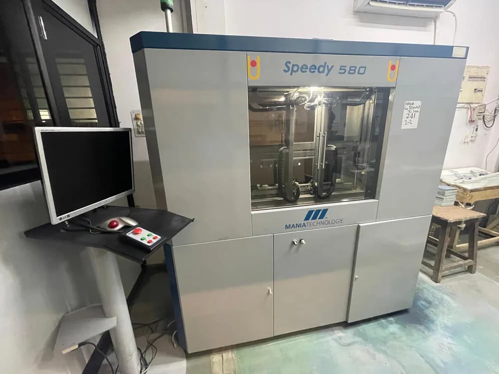
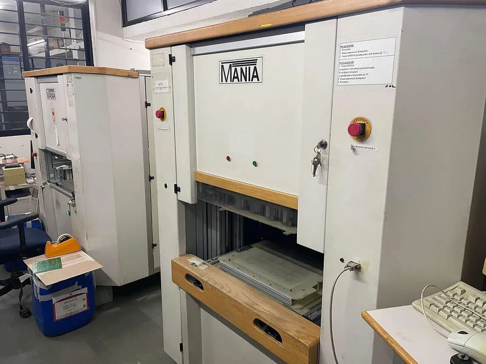
- ISO 9001:2015 across the whole route, every station
- 13 stations, from CAM review to final inspection
- 100% electrical test of every net before packing
- Prototypes and production run the same line
03What we build
Fabrication, assembly, stencils and parts under one roof.
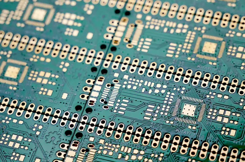
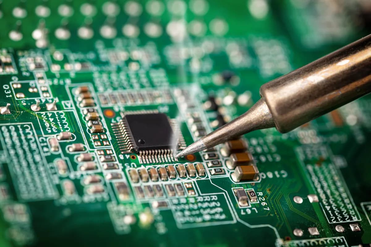
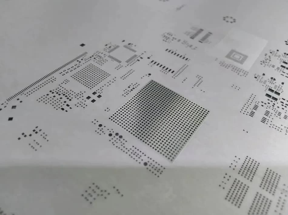
S.B. Electronics is a printed circuit board manufacturer in Gandhinagar, Gujarat. Since 2000 we have made single-sided, double-sided PTH, multilayer (4, 6, 8, 10 and 12 layers) and flexible PCBs in our own plant — and we assemble them, laser-cut their SMT stencils and source their components.
Board types4 constructions
04How to place an order
From spec to paid in five screens.
01/QUOTE
Create the order
Board size, quantity, layers and finish in the instant quote — every dispatch option is priced on screen, live.
02/CART
Add to cart
The priced board lands in your cart with its specification and its Gerber slot, at today's price.
03/CHECKOUT
Check out
Delivery address, billing name and GST number, and a note for our engineers. Nothing to pay at this step.
04/ORDER
Place the order
An order number and its milestones appear immediately; an engineer's DFM review runs before any copper is etched.
05/PAY
Make the payment
Once every board is approved we email the pay link: card or UPI on HDFC Bank's page, a UPI QR to scan, or NEFT/IMPS.
Board specification
- 3 working days₹3,240 incl. GST
- 5 working days₹2,980 incl. GST
- 7 working days₹2,860 incl. GST
- 10 working days₹2,740 incl. GST
01 · QUOTE — Create the order
/quotePayment comes after the review, never at checkout — card or UPI on HDFC Bank's page, a UPI QR, or NEFT/IMPS against the proforma.
05Your board, your spec
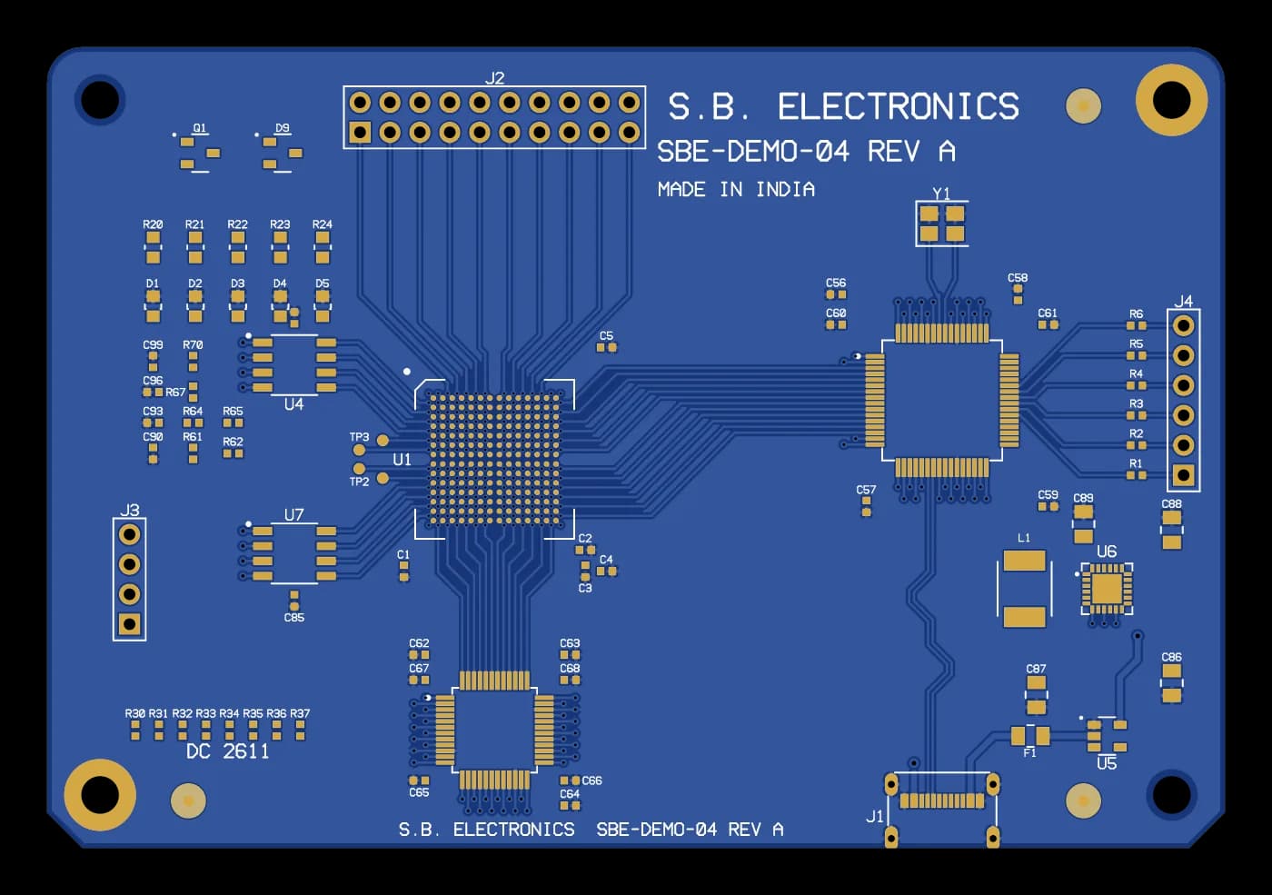
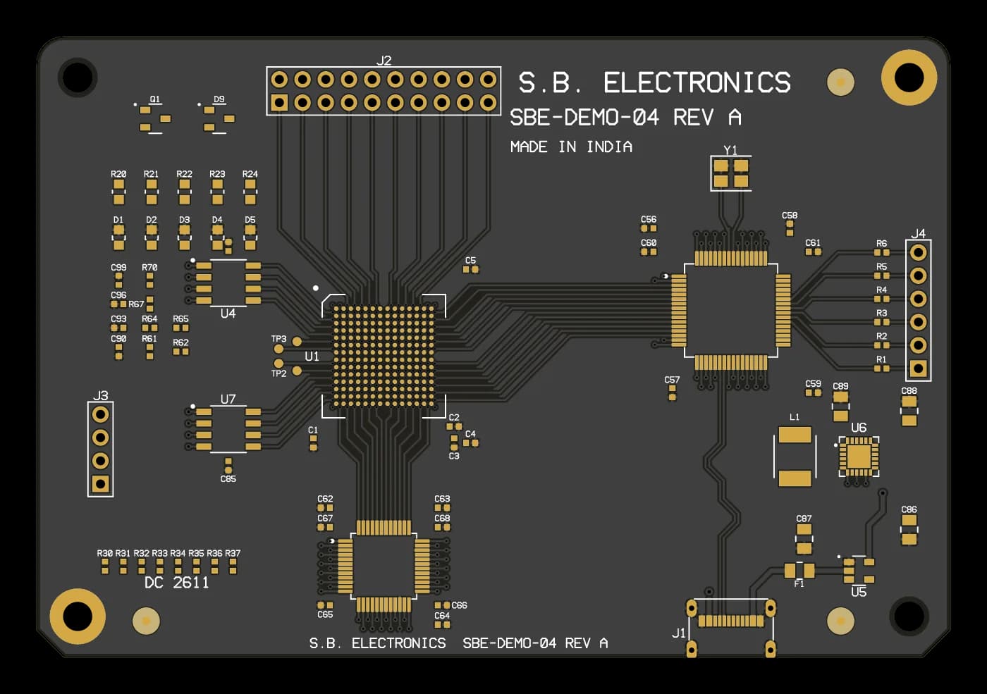
Choose the mask, the finish and the legend.
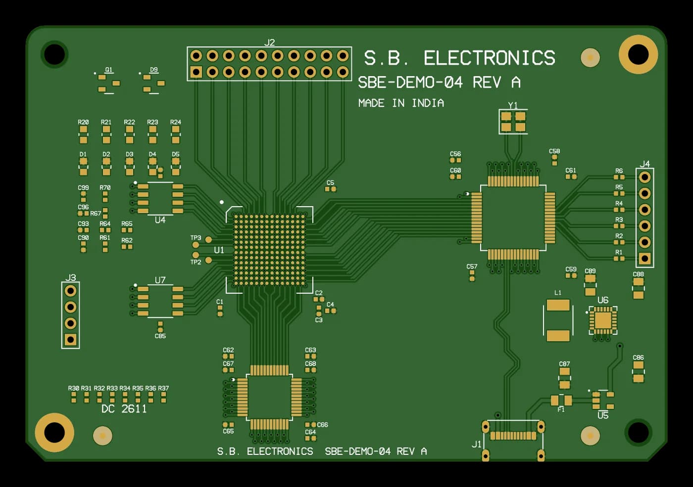
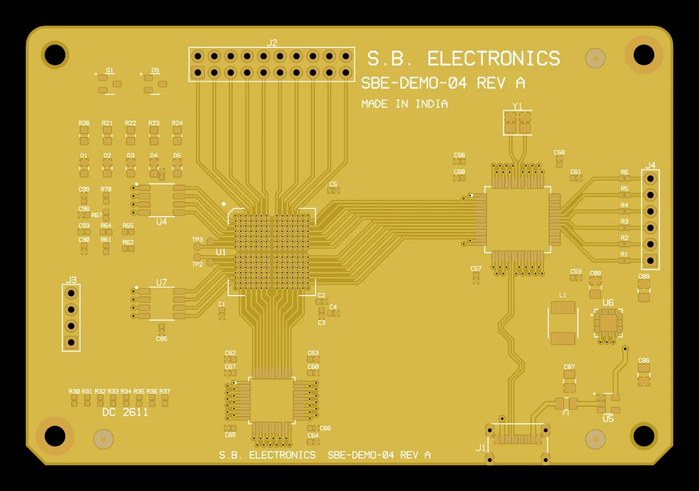
FIG. 02 · SBE-DEMO-04 REV A · top
100.00 × 68.00 mm
U1 · 196-ball BGA, 0.8 mm pitch
Mask Green · Finish ENIG · Legend White
Green mask. The default for a reason: the widest process window, and the clearest contrast between copper, pads and legend for optical inspection.
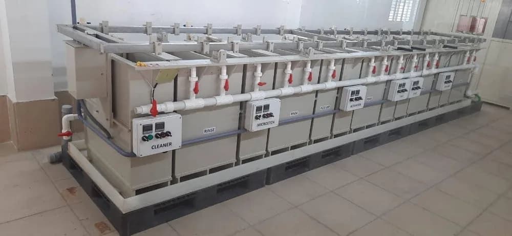
ENIG. Electroless nickel, immersion gold: a flat, solderable pad that suits fine-pitch ICs and BGAs, with a long shelf life. Plated on our own ENIG line.
06From Gerber to dispatch
From Gerber to dispatch, stage by stage.
- CAM
CAM & DFM review
Engineers check your Gerbers, drill and fab notes for manufacturability and prepare the production tooling.
- CNC
CNC drilling
Holes and vias are drilled on CNC machines from your Excellon data.
- PTH
Hole metallisation
Hole walls are made conductive so they can be copper-plated (plated-through holes).
- DRY
Dry film & imaging
Photo-resist film is laminated and the circuit pattern is exposed onto the panel.
- PLT
Copper plating
Copper is electroplated onto the tracks and into the holes to the specified thickness.
- ETC
Etching
Unwanted copper is etched away, leaving the tracks, pads and planes of your design.
- AOI
Automated optical inspection
Every etched layer is scanned against the design data for opens, shorts and nicks.
- LPI
Solder mask
Photo-imageable solder mask is applied, exposed and developed — green or your chosen colour.
- FIN
Surface finish
HASL, lead-free HASL, ENIG or OSP protects the exposed copper and makes it solderable.
- LEG
Legend printing
The silkscreen legend — reference designators, polarity marks, logos — is printed.
- RTG
Routing & V-scoring
Boards are CNC-routed to outline or V-scored into panels, with tabs and rails as specified.
- E-T
Electrical test
100% flying-probe or bed-of-nails test verifies every net for opens and shorts.
- FQC
Final inspection
Final QC against IPC-A-600 acceptance criteria, then protective packing and dispatch.
FIG. 03 · SBE-DEMO-04 REV A · build sequence
Stage 01 / 13CAM · CAM & DFM review
Stage 02 / 13CNC · CNC drilling
Stage 03 / 13PTH · Hole metallisation
Stage 04 / 13DRY · Dry film & imaging
Stage 05 / 13PLT · Copper plating
Stage 06 / 13ETC · Etching
Stage 07 / 13AOI · Automated optical inspection
Stage 08 / 13LPI · Solder mask
Stage 09 / 13FIN · Surface finish
Stage 10 / 13LEG · Legend printing
Stage 11 / 13RTG · Routing & V-scoring
Stage 12 / 13E-T · Electrical test
Stage 13 / 13FQC · Final inspection
FQC · PassIPC-A-600
07Capabilities
The limits engineers ask for first.
| Layer count | 1 to 12 layers |
|---|---|
| Base materials | FR-4 (Tg 150 °C / Tg 170 °C), FR-2, CEM-1, CEM-3, polyimide (flex) |
| Board thickness | 0.4 mm to 3.2 mm standard; 0.2 mm for thin rigid designs |
| Copper weight | 1 oz (35 µm) and 2 oz (70 µm) standard; 3 oz (105 µm) and heavier on request |
| Min. track / space | 6 mil / 6 mil standard; 4 mil / 4 mil fine-line |
| Min. drill diameter | 0.3 mm mechanical; 0.2 mm for fine-pitch designs |
| Surface finish | HASL (leaded), Lead-free HASL, ENIG, OSP |
| Solder mask | Green, Red, Blue, Black, White, Yellow — one or both sides |
| Impedance control | Controlled impedance, ±10% tolerance, with stack-up design support |
| Board size | Minimum 10 × 10 mm; maximum 500 × 600 mm (larger on request) |
| Electrical test | 100% electrical test — flying probe or bed-of-nails fixture — plus AOI |
| Minimum order | No minimum order quantity — one prototype board upwards |
- Assembly
- 0201 parts · 0.4 mm BGA
- Stencils
- 0.08 mm aperture · ±0.01 mm
- Lead time
- 24 h express · 3 / 5 / 7 / 10 days online
08Customers
A few of the companies we make boards for.







- 2,100+customers served since 2000
09Industries
11 industries, from LED drivers to railway signalling.
- 01
LED lighting
Drivers, modules and luminaire boards
Single-sided · white mask
- 02
Automotive and EV
Vehicle electronics, chargers and controllers
Multilayer · heavy copper
- 03
Industrial electronics
Automation, instrumentation and control
Double-sided PTH · LF-HASL
- 04
Renewable energy
Solar inverters, BMS and power conversion
Heavy copper · multilayer
- 05
Medical electronics
Monitoring, diagnostic and lab devices
Multilayer · ENIG
- 06
Telecommunication
Network and infrastructure electronics
Controlled impedance
- 07
Consumer electronics and IoT
Appliances, wearables and connected devices
Fine pitch · ENIG · flex
- 08
Aerospace and defence
High-reliability builds; IPC Class 3 on request
IPC Class 3 on request
- 09
Railways
Signalling, traction and on-board electronics
Class 3 on request · lot traceability
All 11 sectors we build for: automotive, consumer electronics, industrial electronics, IoT, LED lighting, medical electronics, telecommunication, renewable energy, aerospace, railways and defence & security. IoT is covered with consumer electronics, and defence and security with aerospace.
All industries we serve10Quality and testing
Every board is tested before it is packed.
- AOI scan of every etched layer against your design data
- 100% electrical test: flying probe or bed-of-nails fixture — for opens and shorts
- Final inspection to IPC-A-600 acceptance criteria
- IPC-A-610 Class 2 standard workmanship on assemblies; Class 3 on request
- Lot and date-code traceability on every part sourced for assembly
11Ordering online
How do I order PCBs online?
01 · QUOTE
Price it instantly
Enter size, quantity, layers and finish in the instant quote. Rigid 1–2 layer boards are priced on screen; anything else goes to an engineer.
02 · UPLOAD
Upload your data
Gerber RS-274X (or X2) plus Excellon drill files; ODB++ accepted. Zip everything into one archive and upload it with your quote.
03 · DFM
Engineering review
A CAM engineer checks the data for manufacturability and raises any query before tooling is made.
04 · BUILD
Manufacture and test
The job runs through all 13 production stages, ending with a 100% electrical test and final inspection.
05 · TRACK
Track and receive
Follow the order in your account until it leaves by courier — in 3, 5, 7 or 10 working days, as you chose.
Instant pricing: rigid 1–2 layer boards. Request a quote for multilayer, flex, assembly, stencils, sourcing, controlled impedance and large volumes.
12Questions
What buyers ask us first.
What does S.B. Electronics manufacture?
Is there a minimum order quantity?
How long does PCB manufacturing take?
Which files do I need to send for a PCB order?
Where is S.B. Electronics located?
Do you also assemble the boards you make?
13Guides
Notes from the CAM desk.
Cost · · 9 min read
How much does a PCB cost in India? Price factors explained
What sets PCB prices in India: area, layers, quantity, material, finish, tolerances and lead time, plus eight ways to lower yours. Price your board online.
Read the guideFabrication · · 8 min read
What is a PTH PCB? Plated through-holes explained
A PTH PCB has copper-plated holes that join its layers. How holes are plated, PTH vs NPTH, hole-wall copper, annular ring and hole sizing. Read the guide.
Read the guideOrdering · · 7 min read
PCB lead time: what drives it and how to shorten it
What sets PCB lead time: layers, process stages, data queries, materials, quantity and assembly, with typical ranges and eight ways to cut it. Plan ahead.
Read the guide
Start a project
Send us your Gerbers. We will take it from there.
Price one- and two-layer boards online in seconds, or send the full data pack — Gerbers, drill, BOM and centroid — and an engineer replies with a reviewed quote.