Industries · Telecommunication
PCB manufacturer for telecommunication equipment
Multilayer boards for switches, routers, fibre access, radio units and the power and monitoring electronics around them. Stack-ups with controlled impedance, agreed with you before fabrication, and ENIG pads flat enough for fine-pitch BGAs. Made in Gandhinagar since 2000.
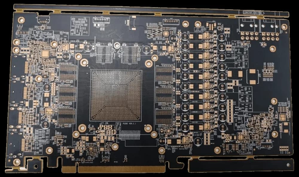
FIG. 01Top layer of a switch line card: 100 Ω pairs from the SFP cages into the switch ASIC, length-matched DDR lanes, the −48 V power train and the stack-up behind it. The dashes are traffic.
- L1 signal
- ENIG pads
- Power pour
- Component outline
- Layers
- 4–12
- Impedance control
- ±10%
- Fine line
- 4 / 4 mil
- Finish for BGAs
- ENIG
01Overview
What do telecom boards need from a PCB maker?
Telecom equipment moves data at rates where a copper track stops behaving like a wire and becomes a transmission line. Its width, the dielectric beneath it and the plane it references set an impedance, and every change along the way reflects part of the signal back towards the transmitter.
That makes the stack-up the real specification. A switch line card, a fibre ONT or a radio unit's digital board is a multilayer, six to twelve layers on most designs, with solid reference planes, differential pairs routed to a target impedance and BGAs that need flat, uniform pads. The power, alarm and monitoring boards around them are simpler, but they share the cabinet and the expectation of years of continuous service.
We agree the stack-up with you before fabrication: layer order, core and prepreg, copper, and the track width for each target impedance. Then we build it the same way every time you reorder.
Last updated
02Board selection
Which boards go into telecom equipment?
| Board in the product | Construction | Base material | Finish | IPC class |
|---|---|---|---|---|
| 01Switch and router line cards | 8–12 layer multilayer | FR-4, Tg 170 °C, controlled impedance | ENIG | Class 2 |
| 02Fibre ONT / OLT and broadband CPE | 4–6 layer multilayer | FR-4, controlled impedance | ENIG | Class 2 |
| 03Radio-unit digital and control boards | 6–8 layer multilayer | FR-4, Tg 170 °C | ENIG | Class 2 |
| 04LTE, NB-IoT and LoRa modem carriers | 4 layer multilayer | FR-4, 50 Ω feed lines | ENIG | Class 2 |
| 05−48 V rectifier, DC-DC and distribution boards | Double-sided or 4 layer | FR-4, 2 oz copper | Lead-free HASL | Class 2 |
| 06Alarm, fan-control and shelf-management boards | Double-sided PTH | FR-4 | Lead-free HASL or ENIG | Class 2 |
Our laminates are FR-4 at Tg 150 °C and Tg 170 °C, which serves digital links and radio designs into the low-gigahertz range with a careful stack-up. PTFE and other low-loss RF laminates are not on our standard list: send the drawing and we will tell you plainly whether we can build it.
03Controlled impedance
Where does a ±10% impedance tolerance go?
- wTrack width
- 0.33 mm
- hHeight above plane
- 0.20 mm
- tCopper thickness
- 35 µm
- εrDielectric constant
- 4.4
- Dielectric height h180–220 µm (±10%)46.2 Ωinside ±10%53.5 Ω
- Track width w305–355 µm (etch ±25 µm)47.7 Ωinside ±10%52.5 Ω
- Dielectric constant εr4.2–4.6 (FR-4 batch and frequency)49.2 Ωinside ±10%50.9 Ω
- Copper thickness t35–50 µm (outer layer plated up)48.3 Ωinside ±10%50.0 Ω
- All four, same directionEvery variable at its worst41.5 Ωoutside ±10%57.0 Ω
N1An estimate, not the final number
Z₀ = 87 / √(εr + 1.41) · ln(5.98 h / (0.8 w + t)), the IPC-2141 surface-microstrip equation. It is good for comparing variables; the agreed stack-up is calculated with a field solver.
N2Solder mask counts too
Mask over a microstrip adds dielectric above the track and pulls the impedance down by a few ohms. It belongs in the calculation, not in the tolerance.
N3What we hold
Controlled impedance, ±10% tolerance, with stack-up design support. Layer order, dielectric thicknesses and the width for each target are agreed before fabrication, then held on every repeat.
04Engineering
Where high-speed boards lose the signal, and how we prevent it
High-speed failures rarely look like broken boards. They look like a link that trains at a lower rate, a port that drops packets when warm, or an EMC test that fails by a few decibels.
- Signal integrity
- EMC
- Lifetime
- Thermal
- Current
P1Signal integrity
Impedance that drifts with the stack-up
Impedance ±10%Why boards fail
A 100 Ω pair designed on a calculator becomes 92 Ω or 110 Ω on the board when the prepreg thickness, copper weight or etched width differs from what the calculator assumed. The reflections close the eye of a high-speed link.
How we handle it
We build controlled impedance to ±10% with stack-up design support. Layer order, dielectric thicknesses and the track width for each target are agreed before fabrication and set for the materials we actually press.
P2EMC
Fast signals over a broken reference plane
Stack-up review before fabricationWhy boards fail
A pair that crosses a split in its reference plane loses its return path. The return current detours, the pair radiates and picks up crosstalk, and the fault in the layout shows up as an EMC failure on the finished product.
How we handle it
Give every fast layer an unbroken neighbouring plane; a 4–12 layer stack-up has room for one. At the stack-up review we point out plane splits under controlled-impedance nets before tooling is made.
P3Lifetime
Uneven pads under a fine-pitch BGA
ENIG · X-ray for BGAWhy boards fail
HASL leaves solder domed and uneven on small pads. Under a 0.8 mm or 0.5 mm pitch BGA, the balls do not all meet the paste at once: open joints, head-in-pillow defects and boards that pass test but fail in the field.
How we handle it
Specify ENIG: a flat nickel-gold surface that solders consistently and stores well. On our assembly line BGAs down to 0.4 mm pitch are placed and then inspected by X-ray.
P4Thermal
Switch ASICs and amplifiers heat the board
FR-4 Tg 170 °CWhy boards fail
A switch ASIC or a radio's power amplifier puts several watts into a small footprint, and in a closed shelf the board is part of the heat path. Laminate softens and plated vias fatigue when a board runs hot for years.
How we handle it
Use Tg 170 °C FR-4 for hot, dense boards, thermal vias under the package into the internal planes, and 2 oz copper on planes that have to spread heat. Copper: 1 oz (35 µm) and 2 oz (70 µm) standard.
P5Current
−48 V power at tens of amps
Copper 1–3 ozWhy boards fail
Telecom shelves run on a −48 V DC bus. Power-entry, rectifier and DC-DC boards carry tens of amps continuously, and a narrow neck in a pour or an undersized connector pad is where they overheat.
How we handle it
Heavy copper and wide pours stitched with plated vias; on a multilayer board, the current shared across two or more internal planes. Copper weights: 1 oz (35 µm) and 2 oz (70 µm) standard; 3 oz (105 µm) and heavier on request.
05Applications
Telecom and network equipment we build for
- A16–12 L · Z₀
Ethernet switches and routers
Switch-ASIC line cards, uplink and SFP interface boards
- A24–6 L
FTTH access equipment
ONT, OLT and media-converter boards
- A36–8 L
Radio and microwave units
Digital, control and power boards around the RF section
- A44 L · 50 Ω
IoT and M2M modems
LTE, NB-IoT and LoRa carriers with 50 Ω feeds
- A52–4 L · heavy Cu
Telecom power systems
−48 V rectifiers, DC-DC converters and distribution
- A62 L
Shelf management and alarms
Monitoring, fan-control and alarm-interface boards
- A76–8 L
Test and network monitoring
Protocol analysers, probes and timing boards
- Not listed?Send the drawing and a line about where the board will be used.Ask an engineer
06Specification
A starting specification for telecom boards
| Construction | 4–12 layers; 6–8 typical for line cardsEven layer counts: 4, 6, 8, 10 and 12 layers |
|---|---|
| Laminate | FR-4 Tg 170 °CPTFE and other RF laminates: ask before design |
| Board thickness | 0.4–3.2 mm1.6 mm default; the stack-up sets it for impedance |
| Copper weight | 1 oz (35 µm) and 2 oz (70 µm) standardOuter layers plated up; 2 oz planes for heat and −48 V current |
| Impedance control | Controlled impedance, ±10% tolerance, with stack-up design supportTypical targets: 50 Ω single-ended, 90 or 100 Ω differential |
| Min. track / space | 6 mil / 6 mil standard; 4 mil / 4 mil fine-line |
| Min. drill | 0.3 mm mechanical; 0.2 mm for fine-pitch designs |
| Annular ring | 0.15 mm minimum for drilled holes (design guideline) |
| Surface finish | ENIG for BGA and fine-pitch boardsAvailable: HASL · LF-HASL · ENIG · OSP |
| Solder mask | Green LPI, included in the impedance calculation |
| Electrical test | 100% electrical test — flying probe or bed-of-nails fixture — plus AOI |
| Assembly | 0.4 mm minimum BGA ball pitch; QFN, QFP and fine-pitch ICsAOI at every stage; X-ray for BGA; functional test on request |
| Components | Authorised distributors and manufacturers only — no grey-market or broker stock |
How to order this spec
Priced online
Simple power, alarm and interface boards (rigid single- and double-sided boards) are priced live: 10 mm to 600 mm per side, 1 to 100,000 boards per line, dispatch in 3, 5, 7 or 10 working days.
Open the instant quoteReviewed by an engineer
Multilayer and impedance-controlled boards, which is most telecom work, are quoted after an engineer reviews the stack-up, and we aim to reply within 24 hours on working days.
Request a quote07Standards context
Which standards apply to telecom equipment?
- IPC-2141A
- Design guide for high-speed controlled-impedance boards
- Impedance equations and test-coupon practice; the source of the microstrip estimate on this page.
- IPC-6012
- Qualification and performance of rigid boards
- Class 2 is the usual build class for telecom equipment; Class 3 on request.
- IEC 62368-1
- Safety of audio/video, information and communication technology equipment
- Insulation and spacing rules for most ICT products, including telecom power.
- Telcordia GR-63-CORE
- NEBS physical protection
- Temperature, humidity, fire-spread and vibration tests for central-office equipment.
- Telcordia GR-1089-CORE
- NEBS EMC and electrical safety
- Lightning surge and power-cross on telecom ports; spacing and copper weight on interface boards follow from it.
- TEC MTCTE
- Mandatory testing and certification of telecom equipment in India
- Certification by the Telecommunication Engineering Centre; it applies to the equipment maker's product.
Stays with you
Product safety (IEC 62368-1), NEBS testing, EMC compliance and TEC certification under MTCTE in India stay with the equipment maker. The board is one component of the tested product.
Comes from us
Boards built to your stack-up and impedance targets (±10%), IPC Class 2 by default and Class 3 on request, with AOI, a 100% electrical test, final inspection to IPC-A-600 and an ISO 9001:2015 certified quality management system.
09FAQ
Telecommunication: common questions
Not covered here? Ask an engineer — we aim to reply within 24 hours on working days.
What PCB is used in telecommunication equipment?
What impedance tolerance can you hold?
Can you make RF boards on Rogers or PTFE laminates?
Why is ENIG preferred for telecom boards?
Who makes telecom PCBs in India?
Telecommunication
Send the stack-up. We will build the impedance you designed.
Upload Gerbers, drill files and your stack-up with the impedance targets and the nets they apply to. An engineer reviews them and replies with a quote and any stack-up questions.