Industries · Consumer electronics and IoT
PCB manufacturer for consumer electronics and IoT
Boards for appliances, wearables, smart-home devices and wireless modules — products designed backwards from a unit price and an enclosure. Single-, double-sided and four-layer FR-4, flex and assembly, from the first ten prototypes to the production run.
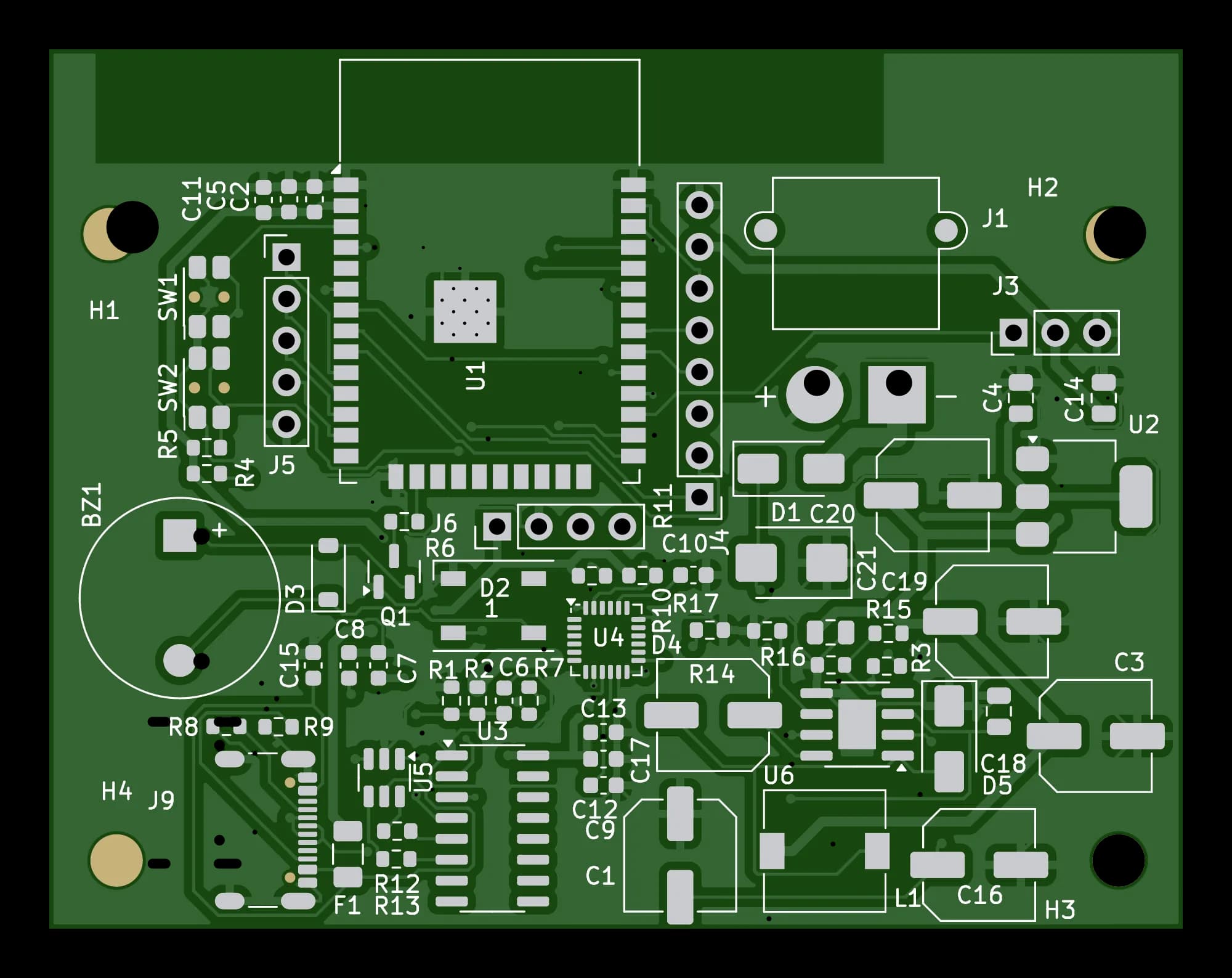
- 1Antenna keep-out — no copper on any layer, and none added in CAM.
- 2Via fence — stitches the top pour to the L2 ground plane.
- 350 Ω feed, π match — 0201 parts, tuned on the prototype.
- 4QFN on ENIG — flat pads for fine pitch; BGAs to 0.4 mm.
- 5Fiducials, test pads — placement marks; SWD pads for programming.
- Fine line
- 4 / 4 mil
- Smallest part
- 0201
- BGA pitch
- 0.4 mm
- Minimum order
- None
01Overview
What does a consumer or IoT product ask of its PCB?
A consumer product is designed backwards from a price and a box. A smart plug, a fitness band or a Wi-Fi sensor ships in thousands, so a few square centimetres of laminate, one extra layer pair or a finish nobody needed is paid for again on every unit.
Most of these products sit on a handful of constructions: single- and double-sided FR-4 for appliance control, chargers and remotes; four layers for anything with a radio, because a ground plane under the RF line keeps the antenna match and the regulator's noise under control; thin boards and flex where the enclosure is tight.
Appliance and consumer brands order from us alongside start-ups and design houses. A first batch of ten prototypes and a repeat order of thousands run on the same line, through the same checks.
Last updated
Consumer brands on our customer list
- Bajaj Electricals
- Philips
- Syska
02Board selection
Which boards go into consumer and IoT products?
| Board in the product | Construction | Base material | Finish | IPC class |
|---|---|---|---|---|
| 01Appliance control and display boards | Double-sided PTH | FR-4 | Lead-free HASL | Class 2 |
| 02Chargers, adaptors and small power supplies | Single-sided | FR-4, CEM-1 or FR-2 | Lead-free HASL or OSP | Class 2 |
| 03Smart plugs, switches and lighting controllers | Double-sided PTH | FR-4 | OSP or lead-free HASL | Class 2 |
| 04Wi-Fi, BLE and LoRa modules and sensor nodes | 4 layer multilayer | FR-4, 0.8–1.6 mm, controlled impedance | ENIG | Class 2 |
| 05Wearables and hearables | Thin multilayer + flex | Thin FR-4; polyimide flex | ENIG | Class 2 |
| 06Gateways, hubs, set-top and audio boards | 4–6 layer multilayer | FR-4, controlled impedance | ENIG | Class 2 |
Wireless boards are often smaller than the 50 × 50 mm our assembly line takes as a single board, so they are built and assembled as arrays: V-scored or tab-routed, with rails, fiducials and tooling holes for your SMT line or ours.
03Engineering
Consumer and IoT board problems, and how we solve them
Small, cheap and wireless pull against each other. These are the trade-offs we see on every consumer design, and what we do in the build.
- Cost
- Signal integrity
- EMC
- Thermal
- Lifetime
P1Cost
The unit price is set on the panel
DFM review before toolingWhy boards fail
At volume a bare board's price is mostly laminate area and process steps. An outline a few millimetres too big for an efficient array, a layer pair the routing did not need, or gold on a board of through-hole parts is paid for again on every unit.
How we handle it
Send the design before it is frozen. CAM review looks at how the outline nests in the array, and we suggest the cheapest construction that still meets the layout: two layers where routing allows, OSP or lead-free HASL where ENIG buys nothing.
P2Signal integrity
The antenna is tuned to the copper around it
Impedance ±10% · keep-outs heldWhy boards fail
A trace or chip antenna is matched for the ground and dielectric beside it. A ground pour, via or battery clip that creeps into the keep-out — or a different laminate thickness on the repeat order — detunes it. Range drops and nobody can say why.
How we handle it
We hold keep-outs exactly as drawn, on every layer, and add no balancing copper inside them. Stack-ups are built to the agreed dielectric thicknesses with controlled impedance to ±10%, so the match tuned on the prototype holds in production.
P3EMC
A regulator and a radio on 30 mm of board
4 L · solid L2 groundWhy boards fail
Battery products put a DC-DC converter, a microcontroller, a radio and a USB port within millimetres of each other. On two layers return currents wander, switching noise reaches the receiver, and ESD from the USB shell finds a way into the logic.
How we handle it
Four layers with an unbroken ground on L2 give every signal a short return path and screen the RF section from the regulator. We build 4, 6, 8, 10 and 12 layers and help with the stack-up, so the planes sit where your layout needs them.
P4Thermal
Thin boards and fine pitch leave no margin in reflow
0201 · 0.4 mm BGA · X-rayWhy boards fail
A 0.8 mm board with a fine-pitch BGA on one side and a coin-cell holder on the other bows in the reflow oven. Bow lifts the package's edge balls, and an uneven finish leaves 0201 parts tombstoned or bridged.
How we handle it
ENIG gives flat, solderable pads for fine pitch; balanced copper on opposite layers and an array with rails keep thin boards flat through reflow. Our line places 0201 parts and 0.4 mm-pitch BGAs, and X-rays the joints nobody can see.
P5Lifetime
A product sells for years; its parts don't
EOL / NRND reviewWhy boards fail
Consumer designs stay in production for years while the radio, sensor or regulator they were designed around goes end-of-life or into allocation. Found late, a missing part stops the line.
How we handle it
Every BOM we source gets a review for availability, lifecycle (EOL / NRND) and cost, and drop-in cross-references are proposed for your approval. Authorised distributors and manufacturers only — no grey-market or broker stock.
04Stack-up
Why most radio boards have four layers
Trace width W≈ 2.85 mm
Height to ground h1.53 mm
Trace width W≈ 0.33 mm
Height to ground h0.20 mm
- Reference plane
- Bottom copper, 1.53 mm down
- L2 ground, 0.20 mm down
- 50 Ω microstrip width
- ≈ 2.85 mm — wider than the radio's RF pin
- ≈ 0.33 mm — about the width of an 0201 part
- Where the field goes
- Wide: it couples into neighbouring traces and parts
- Tight to the trace, over the plane
- Return path
- Wherever the bottom pour happens to be continuous
- An unbroken plane under every signal
- When it is the right choice
- Simple radios with a grounded coplanar feed and generous pour
- Most Wi-Fi, BLE and LoRa products
Widths from the IPC-2141 microstrip approximation, FR-4 at εr 4.3, 35 µm copper; your field solver has the last word. We build to the stack-up you modelled, with controlled impedance to ±10%.
05Applications
Consumer and IoT products we build for
- A11–2 L
Home appliances
Washing-machine, air-conditioner, fan, mixer and water-purifier controllers
- A21–2 L
Chargers and adaptors
Phone chargers, adaptors, battery chargers and power banks
- A32–4 L
Smart home
Smart plugs, switches, lighting controllers, locks and doorbells
- A44 L rigid · flex
Wearables and hearables
Fitness bands, smartwatches and earbud charging cases
- A54 L · RF
IoT sensors and trackers
Wi-Fi, BLE, LoRa and cellular nodes, asset trackers and smart meters
- A62–6 L
Audio and entertainment
Speakers, amplifiers, soundbars and set-top boxes
- A71–2 L
Remotes, toys and keypads
Remote controls, toys and keypad interface boards
06Specification
A starting specification for IoT boards
| Construction | 4 layers (signal / ground / power / signal) for radio boards; 1–2 layers for appliance and power boardsRange: 1 to 12 layers |
|---|---|
| Laminate | FR-4; CEM-1 or FR-2 for single-sided cost-down boardsAvailable: FR-4 (Tg 150 °C / Tg 170 °C), FR-2, CEM-1, CEM-3, polyimide (flex) |
| Board thickness | 0.8–1.0 mm for wearables and modules; 1.6 mm elsewhereRange: 0.4 mm to 3.2 mm standard; 0.2 mm for thin rigid designs |
| Copper weight | 1 oz (35 µm) on outer layers1 oz (35 µm) and 2 oz (70 µm) standard; 3 oz (105 µm) and heavier on request |
| Min. track / space | 6 mil / 6 mil standard; 4 mil / 4 mil fine-line |
| Min. drill | 0.3 mm mechanical; 0.2 mm for fine-pitch designs |
| Impedance control | Controlled impedance, ±10% tolerance, with stack-up design supportState 50 Ω single-ended for the RF feed, and the nets it applies to |
| Surface finish | ENIG for modules and fine pitch; OSP or lead-free HASL for cost-driven boardsAvailable: HASL · LF-HASL · ENIG · OSP |
| Mask and legend | Green mask, white legend; black or white mask for boards seen through the enclosureMask colours: Green, Red, Blue, Black, White, Yellow |
| Delivery | Arrays with rails, fiducials and tooling holesV-score, tab-routing (mouse bites) or a combination; rails, fiducials and tooling holes |
| Electrical test | 100% electrical test — flying probe or bed-of-nails fixture — plus AOI |
| Assembly | SMT, through-hole (THT) and mixed technology; 0201 parts, 0.4 mm BGAFull turnkey (we source the parts), partial turnkey or consigned (you supply them) |
Standards context
Which standards apply to consumer and IoT products?
Consumer devices are approved as finished products. These are the approvals most makers selling in India work through, and where the PCB enters each.
- IEC 62368-1
- Safety of audio/video, information and communication technology equipment
- Replaced IEC 60065 and 60950-1; sets the creepage, clearance and fire rules a charger or adaptor board is laid out to.
- IEC 60335-1
- Safety of household and similar electrical appliances
- The appliance's own safety standard; the control board's spacing and materials are assessed as part of it.
- BIS CRS
- Compulsory registration for electronics sold in India
- Applies to the finished product — adaptors, power banks, smart speakers and more — not to the bare board.
- WPC ETA
- Equipment type approval for radio devices in India
- Needed for Wi-Fi, BLE and LoRa products; antenna performance is measured on the finished device, so the board must match the one that was tested.
- E-Waste Rules 2022
- India's limits on hazardous substances in electrical and electronic equipment
- RoHS-style limits on lead and other substances; lead-free HASL, ENIG and OSP finishes help the product meet them.
- Comes from us
- Boards built to IPC Class 2 to your drawing and stack-up, with lead-free finishes, a 100% electrical test, final inspection to IPC-A-600 and an ISO 9001:2015 certified quality management system.
Stays with youProduct safety (IEC 62368-1 or IEC 60335-1), BIS registration, WPC approval for radios and EMC testing stay with the brand that sells the device. The board is one component of the tested product.
How to order this spec
Priced online
Single- and double-sided boards for appliances, chargers and switches are priced in the instant quote — 10 mm to 600 mm per side, 1 to 100,000 boards per line — with dispatch in 3, 5, 7 or 10 working days.
Open the instant quoteReviewed by an engineer
Four-layer radio boards, impedance targets, flex, assembly and volume schedules go to an engineer, who aims to reply within 24 hours on working days.
Request a quote08FAQ
Consumer electronics and IoT: common questions
Not covered here? Ask an engineer — we aim to reply within 24 hours on working days.
What PCB is used in consumer electronics and IoT devices?
Who makes IoT PCBs in India?
Do I need four layers for a Wi-Fi or Bluetooth board?
Can you build small batches of IoT prototypes?
Can you assemble 0201 parts and fine-pitch BGAs?
Consumer electronics and IoT
Send the design. We will build the board your antenna was tuned on.
Upload Gerbers, drill files, the stack-up and the BOM. An engineer checks keep-outs, impedance targets and the array layout and replies with a quote; simple double-sided boards can be priced online straight away.