On this page · 9 sections
- 01What is PCB lead time?
- 02How long does it take to make a PCB?
- 03Where do the days go?
- 04What makes a PCB order take longer?
- 05How does your data affect lead time?
- 06How can you shorten PCB lead time?
- 07Is 24-hour express manufacturing worth it?
- 08How do prototype and production lead times differ?
- 09How do you plan a PCB order around a deadline?
Building this board?
After the price, the next question on every order is when the boards will arrive. The answer depends less on how fast the factory works than on what the board is, what data arrives with it and what has to be bought in. This guide walks through where the days go between upload and dispatch, which of them you control, and how to plan prototypes and production around a deadline.
What is PCB lead time?
PCB lead time is the number of working days between an approved order and the dispatch of finished boards. Three details catch buyers out. It counts working days, not calendar days — ours run Monday to Saturday. It ends at dispatch, so courier transit comes on top. And it starts when the order is confirmed and the data has cleared CAM review, not at the moment of upload: a file that raises a query waits until the query is answered.
How long does it take to make a PCB?
Lead time grows with the construction. The ranges below are typical for the industry, in working days before transit; the right-hand column gives ours.
Table 1 · Typical PCB lead times by construction
| Construction | Typical industry range | At S.B. Electronics |
|---|---|---|
| Single- and double-sided, quick-turn | 2–5 working days | 3, 5, 7 or 10 working days, priced in the instant quote; 24 h express for urgent simple prototypes |
| Single- and double-sided, standard | 5–10 working days | Choose the dispatch option that fits your schedule |
| Multilayer, 4 to 12 layers | 7–15 working days | Quoted per job after engineering review |
| Flexible circuits | Longer than rigid: coverlay and stiffener tooling | Quoted per job |
| PCB assembly | Board lead time plus parts procurement and assembly | Quoted per job, after a BOM review |
| Imported boards | 7–15 days manufacturing, plus shipping and customs | — |
Industry ranges are typical published figures, not guarantees. Transit is extra in every case.
24 h express
Urgent simple prototypes, by arrangement
3 working days
Fastest online option
5 working days
Online option
7 working days
Online option
10 working days
Economy online option
Quoted jobs
Multilayer, flex, assembly
Quoted per job after engineering review
Where do the days go?
A double-sided PTH board passes through 13 stages on our floor, in this order. None of them takes long on its own; the time is in the sequence, the queue at each line and the batching of chemistry.
- CAM & DFM review. Engineers check your Gerbers, drill and fab notes for manufacturability and prepare the production tooling.
- CNC drilling. Holes and vias are drilled on CNC machines from your Excellon data.
- Hole metallisation. Hole walls are made conductive so they can be copper-plated (plated-through holes).
- Dry film & imaging. Photo-resist film is laminated and the circuit pattern is exposed onto the panel.
- Copper plating. Copper is electroplated onto the tracks and into the holes to the specified thickness.
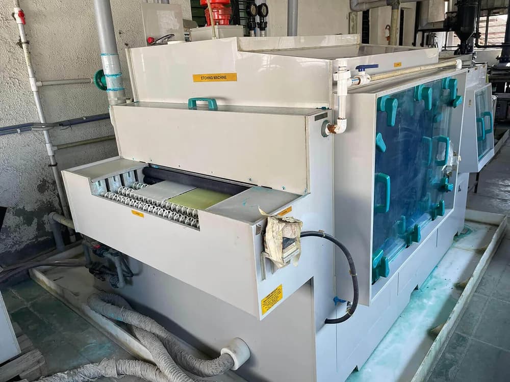
- Etching. Unwanted copper is etched away, leaving the tracks, pads and planes of your design.
- Automated optical inspection. Every etched layer is scanned against the design data for opens, shorts and nicks.
- Solder mask. Photo-imageable solder mask is applied, exposed and developed — green or your chosen colour.
- Surface finish. HASL, lead-free HASL, ENIG or OSP protects the exposed copper and makes it solderable.
- Legend printing. The silkscreen legend — reference designators, polarity marks, logos — is printed.
- Routing & V-scoring. Boards are CNC-routed to outline or V-scored into panels, with tabs and rails as specified.
- Electrical test. 100% flying-probe or bed-of-nails test verifies every net for opens and shorts.
- Final inspection. Final QC against IPC-A-600 acceptance criteria, then protective packing and dispatch.
A multilayer board adds a whole cycle before drilling. Each inner layer is imaged, etched and inspected, given an oxide treatment for resin adhesion, then stacked with prepreg and pressed under heat and vacuum. The press cycle alone holds the stack at temperature for an hour or two, and every inner layer must be finished before it starts. That is why a four-layer board takes days longer than a two-layer one of the same size.
At the other end, a single-sided board and a double-sided NON-PTH board skip hole metallisation and copper plating altogether, which makes them the quickest constructions to turn round. Flexible circuits follow a similar sequence on polyimide film, with a coverlay laminated in place of liquid solder mask and stiffeners bonded afterwards — extra steps that each need their own tooling.
What makes a PCB order take longer?
Table 2 · What adds time, and what you can do about it
| Factor | Why it adds time | What you can do |
|---|---|---|
| Incomplete or ambiguous data | CAM raises a query and the job waits for your answer | Send a complete data pack with a fab note |
| Layer count | Inner layers and lamination run before drilling | Use the layers the design needs — no more, no fewer |
| Non-standard material | High-Tg, unusual thickness, heavy copper or polyimide may have to be bought in | Choose stocked materials; ask early about anything else |
| Special requirements | Controlled impedance needs stack-up approval, coupons and TDR; Class 3 needs microsections | Put every requirement in the first enquiry, not after the order |
| Quantity | More panels through every stage; longer plating and test runs | Order prototypes first and plan production volumes ahead |
| Test method | A bed-of-nails fixture must be built before volume testing | Flying probe for prototypes; build the fixture once for repeat volume |
| Assembly | Component lead times often exceed the board's | Order long-lead parts early and approve alternates |
| Changes after release | A revised file restarts CAM review | Freeze the revision before you order |
How does your data affect lead time?
More than any machine does. Every order starts with a CAM engineer checking the Gerbers, drill data and fab note against our process limits. Clean data passes straight through. Ambiguous data — a missing outline, plated and non-plated holes merged, units that disagree, a note that contradicts the files — produces an engineering query, and the job stands still until it is answered. We raise one consolidated query with a proposed fix rather than a series of questions, but the clock still waits for your reply.
Two habits remove most of that delay: check the data pack in a Gerber viewer before upload, and name a contact who can answer a technical question the same day. Our Gerber preparation guide and DFM checklist list what CAM looks for.
How can you shorten PCB lead time?
- Send complete data. Gerbers, drill files, a closed outline and a fab note, in one zip, from the latest revision.
- Design to standard capabilities. 6 mil / 6 mil track and space and 0.3 mm drills sit inside our standard process window; finer limits narrow it and slow some stages. Check our capabilities before layout.
- Choose standard materials and finishes. FR-4 at standard thickness and copper, with HASL, lead-free HASL, ENIG or OSP, is what the line runs every day.
- Answer queries the same day. A query answered in an hour costs an hour; one answered next week costs a week.
- Pay for speed only on the critical path. Pick the dispatch option the schedule needs, not the fastest one by habit.
- Order parts early for assembly. Long-lead components, not the board, usually set the date for PCB assembly. Approve alternates before the order, or let us source to a reviewed BOM — see component sourcing.
- Keep revisions stable for repeat orders. An unchanged revision reuses its CAM tooling, so a repeat order clears review faster.
- Buy locally when time matters. A domestic order avoids international shipping and customs clearance, and queries are answered in your own working day.
Is 24-hour express manufacturing worth it?
Sometimes. We offer 24-hour express for urgent simple prototypes, by arrangement: standard single- and double-sided boards with clean data. It is worth it when a board is the only thing blocking a bring-up, a demonstration or a production line, and waiting costs more than the express charge. It is rarely worth it for a design that will change next week. Multilayer, flex and assembled work need their full process sequence, so their lead time is quoted per job.
How do prototype and production lead times differ?
A prototype order is a few panels tested by flying probe, and its lead time is mostly the fixed sequence of stages. A production order runs many more panels through every stage — plating, etching, test and inspection all take longer — and may need a test fixture built first. Plan production after the prototype is approved, on the same revision, and share a forecast if volumes will repeat, so materials can be planned before the order arrives.
How do you plan a PCB order around a deadline?
Work backwards from the date the boards must be on the bench:
- Subtract courier transit to your site.
- Subtract the dispatch option or quoted lead time, counted in working days — Sundays and public holidays do not count.
- For assembly, subtract the longest component lead time, unless the parts are already in stock.
- Subtract a day for data review and any query.
- The result is the latest date to place the order with approved data. If it has already passed, that is when paying for speed makes sense.
For rigid one- and two-layer boards, the instant quote shows each dispatch option with its price, so you choose the date and the cost together. For everything else, send the data through our contact page; we aim to reply within 24 hours on working days with a reviewed quote and a lead time. An order can be cancelled within 2 hours of ordering, before manufacturing starts — after that, the clock is running.
Written by
S.B. Electronics Engineering Team
The CAM, production and quality engineers at our factory in the Gandhinagar G.I.D.C. Electronics Estate — the people who review incoming data and build the boards. Published .