On this page · 9 sections
- 01What files are needed to manufacture a PCB?
- 02What is a Gerber file?
- 03How do you export Gerbers from KiCad, Altium or EasyEDA?
- 04Which layers and file names should the zip contain?
- 05What are the most common Gerber export mistakes?
- 06What should a fab note include?
- 07How do you check Gerber files before uploading them?
- 08What happens to your files after you upload them?
- 09Gerber checklist before you upload
Building this board?
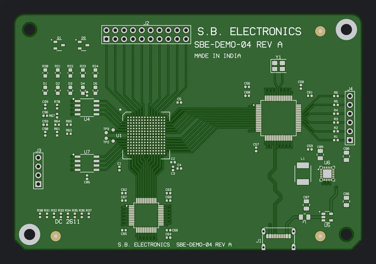
A Gerber file set is the manufacturing drawing of your board, split into one image per layer. Clean data goes straight into CAM. Incomplete data starts an engineering query that holds your job until you answer it — often a day or more of lead time lost before a panel is cut. This guide covers what a fabricator needs, how to export it from the common CAD tools, and the mistakes we see most often at our CAM desk in Gandhinagar.
What files are needed to manufacture a PCB?
A bare board needs three things: the layer images (Gerber), the holes (Excellon drill data) and the construction details that images cannot carry (a fab note or drawing). Assembly adds a bill of materials and a centroid file. The formats we accept: Gerber RS-274X (or X2) plus Excellon drill files; ODB++ accepted. For assembly: add a BOM (CSV / Excel, with manufacturer part numbers) and centroid / pick-and-place data.
Table 1 · The manufacturing data pack
| File | Format | What it tells the fabricator | Needed for |
|---|---|---|---|
| Copper layers (top, inner, bottom) | Gerber X2 / RS-274X | Tracks, pads and planes on each layer | Every board |
| Solder mask (top, bottom) | Gerber | Openings in the mask over pads | Every masked board |
| Legend / silkscreen | Gerber | Designators, polarity marks, logos | Boards with a legend |
| Solder paste (top, bottom) | Gerber | Stencil apertures | Stencils and assembly |
| Board outline | Gerber, its own file | Routed profile, slots and cut-outs | Every board |
| Drill — plated and non-plated | Excellon | Hole positions, sizes and plating | Every board with holes |
| Fab note or drawing | PDF or text | Stack-up, thickness, finish, colours, class | Every board |
| Netlist | IPC-D-356 | Design-intent connectivity for electrical test | Recommended |
| BOM and centroid | CSV / Excel | Parts, designators, X/Y, rotation, side | Assembly |
Scroll the table sideways →
L1 · .GTL
Top copper
L2 · .G1
Inner — ground
L3 · .G2
Inner — power
L4 · .GBL
Bottom copper
SM · .GTS
Top solder mask
LG · .GTO
Top legend
NC · .DRL
Excellon drill
OL · .GKO
Board outline
What is a Gerber file?
A Gerber file is a 2D vector image of one board layer, written in a plain-text format maintained by Ucamco. Extended Gerber (RS-274X) embeds its aperture definitions in each file. The older RS-274D needed a separate aperture list and is obsolete — do not send it. Gerber X2 adds attributes on top of RS-274X: each file declares its own function (top copper, plated drill, profile) and pads can carry net and component data. X2 is backward compatible, so any fabricator that reads RS-274X reads X2.
ODB++ and IPC-2581 go further: one structured package with layers, drill, stack-up and netlist together. We accept ODB++. Whatever the format, the rule is the same — send manufacturing output, not the design database. A native board file (.kicad_pcb, .brd, .PcbDoc) opened in a different version of the tool can render differently, so treat it as a reference, never as the data we build from.
How do you export Gerbers from KiCad, Altium or EasyEDA?
Every mainstream tool exports Gerbers in a few clicks. The settings below are the ones that matter; the rest can stay at their defaults.
KiCad
- Refill all copper zones first (press B in the PCB editor) and run the design rules checker, so the pours you export match the final design.
- Choose File → Fabrication Outputs → Gerbers. Tick every copper layer, both mask layers, both silkscreen layers, both paste layers and Edge.Cuts.
- Keep Use extended X2 format ticked and tick Generate Gerber job file — the job file tells CAM the layer order.
- Click Generate Drill Files: Excellon format, millimetres, and leave PTH and NPTH in single file unticked so plated and non-plated holes stay separate.
Altium Designer
- File → Fabrication Outputs → Gerber Files. Set units to millimetres and format to 4:4 (or 2:5 in inches) for full resolution.
- On the Layers tab, plot every used layer plus the mechanical layer that carries the board outline. Do not mirror any layer.
- File → Fabrication Outputs → NC Drill Files with the same units and format, generating separate files for plated and non-plated holes.
- Export an IPC-D-356A netlist from the same output job, so the electrical test compares the board against your design intent.
EasyEDA, Eagle, OrCAD and others
Every other tool has a fabrication or CAM menu that writes a Gerber-plus-drill set. Whichever tool you use, check three things after export: the outline file is present, the drill file is present, and the drill file uses the same units as the Gerbers.
Which layers and file names should the zip contain?
File names are not standardised, but consistent names prevent misreads. Gerber X2 files declare their own function; with plain RS-274X, CAM relies on the name. Most tools can write the Protel-style extensions below, which every CAM system recognises.
Table 2 · Common Gerber file extensions
| Layer | Typical extension | Notes |
|---|---|---|
| Top copper | .GTL | L1 — the component side |
| Inner layers | .G1, .G2 … (.GP1 for planes) | Name them L2, L3 … in stack order |
| Bottom copper | .GBL | The last layer in the stack |
| Top / bottom solder mask | .GTS / .GBS | Defines openings, not the mask itself |
| Top / bottom legend | .GTO / .GBO | Keep it off pads |
| Top / bottom paste | .GTP / .GBP | Becomes the stencil apertures |
| Board outline | .GKO or .GM1 | One closed contour |
| Drill, plated and non-plated | .DRL / .TXT | Excellon, with a tool table |
What are the most common Gerber export mistakes?
Seven mistakes account for almost every data query we raise. Each takes a minute to fix before upload and much longer after, because the job waits for your answer.
- No board outline, or an outline drawn on the legend or a copper layer. The profile must be its own closed contour; a gap in it means CAM cannot route the board.
- Missing drill file. Pads in the copper Gerbers are not holes. Without Excellon data we would be guessing sizes and positions — and we will not guess.
- Plated and non-plated holes merged with no way to tell them apart. Mounting holes come back plated, or component holes come back bare.
- Inner planes with unclear polarity. Some tools write power planes as negative images. Name them clearly so CAM reads them the right way round.
- Unit or format mismatch between the Gerbers and the drill file. Holes land in the wrong place on screen and the job stops until it is resolved.
- Stale or mixed revisions. One layer re-exported after an edit and the others not. Re-export the complete set every time.
- Mirrored bottom layers. Export every layer as seen from the top. The fabricator handles any mirroring.
What should a fab note include?
Gerbers describe geometry, not construction. A one-page fab note — a README or a PDF drawing in the same zip — removes the guesswork. State at least:
- Layer count and stack-up order, with each inner layer named by its file.
- Finished board thickness and tolerance — 1.6 mm is the industry default if nothing is stated.
- Copper weight per layer. We build 1 oz (35 µm) and 2 oz (70 µm) as standard; 3 oz (105 µm) and heavier on request.
- Base material and Tg class — FR-4 Tg 150 °C or Tg 170 °C covers most designs; say which.
- Surface finish (HASL, lead-free HASL, ENIG or OSP) and the solder-mask and legend colours.
- IPC class, and any controlled-impedance targets with their layers and tolerance.
- Special features: castellated holes, countersinks, slots, and whether you want a V-scored or tab-routed panel.
How do you check Gerber files before uploading them?
Open the zip in a Gerber viewer — not in your CAD tool. KiCad's GerbView, gerbv or any online viewer shows exactly what a fabricator sees. Five minutes here saves a day of queries.
- Load every file and confirm the layers line up on one origin.
- Turn on the drill layer over the copper: every pad that should have a hole has one, and nothing else does.
- Check the outline is closed and that copper stops short of it.
- Inspect both mask layers: every pad has an opening, and fine-pitch rows keep a mask dam between pads where you want one.
- Read the legend: no text over pads, polarity marks visible, revision and date code present.
Then zip the set under a name that carries the project and revision — controller-v2r1-fab.zip, for example — and keep one archive per revision. Upload it with an instant quote for a one- or two-layer board, or send it through our contact page for multilayer, flex and assembly work.
What happens to your files after you upload them?
At S.B. Electronics a CAM engineer imports the set, compares it with the fab note and checks it against our manufacturing capabilities: track and space, drill sizes, annular ring, mask clearances and outline. Panelisation, etch compensation, test coupons and tooling holes are added in CAM, so you never need to draw them. If anything is ambiguous, we raise one consolidated query with a proposed fix rather than a series of questions, and we do not change your design without your confirmation. Once the data is clear it goes to drilling, imaging and the rest of the PCB fabrication process.
Gerber checklist before you upload
- Every copper layer, in stack order, named L1 … Ln.
- Top and bottom solder mask; legend and paste layers if used.
- One closed board outline in its own file.
- Excellon drill data with plated and non-plated holes separated, in the same units as the Gerbers.
- A fab note with layers, thickness, copper, material, finish, colours and class.
- An IPC-D-356 netlist (recommended).
- BOM and centroid data if we are assembling the board.
- Everything re-exported after the last edit, checked in a viewer and zipped as one archive.
Written by
S.B. Electronics Engineering Team
The CAM, production and quality engineers at our factory in the Gandhinagar G.I.D.C. Electronics Estate — the people who review incoming data and build the boards. Published ; last reviewed and updated .